|
AES Makers (A-Z order) AES Systems |
|||||||
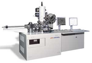 |
JEOL JAMP-9500F AES made in Japan |
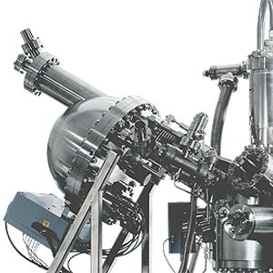 |
Omicron Nanotechnology NanoSAM made in Germany |
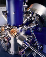 |
Thermo-Fisher 350F AES made in England |
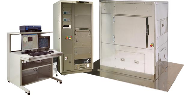 |
Ulvac-PHI 700 Auger Nanoprobe made in USA |
JAMP-9500F The electron spectrometer is an electrostatic hemispherical analyzer (HSA) with a multi-channel detector, and was optimally designed for Auger analysis. It provides extreme energy resolution without sacrificing sensitivity. With the JAMP-9500F, high resolution SEM imaging is possible as well as Auger image analysis and line profile analysis. Also, depth profile analysis can be performed during ion etching. The JAMP-9500F features a high performance ion gun for high speed sputtering and low energy charge neutralization. User-friendly and easily operated, the JAMP-9500F also offers the flexibility of optional analysis functions such as EDS, SIMS and XPS. Features
|
NanoSAM In contrast to other Auger tools the extremely good resolution is not only available at standard 20kV beam energy, but even at 5 keV the SAM resolution remains below 10 nm. This allows operation in a parameter range where the Auger cross sections are high, and well documented for quantitative analysis. The NanoSAM Lab is tailored for the fast and efficient acquisition of data on routine samples, while maintaining the flexibility to operate in untypical parameter ranges on challenging materials. Furthermore, the NanoSAM Lab may be extended with additional techniques for a complementary analysis of the key sample characteristics, for example the crystal structure (EBSD), or the magnetic domain structure (SEMPA) |
350F Product detail: High-performance scanning Auger electron spectrometer (AES)
|
PHI 700 Nanoprobe The 700’s Schottky field emission optics provide Auger spatial resolution of less than 8 nm. The result is rapid, high resolution secondary electron and Auger imaging of submicron features. The coaxial geometry of the 700’s electron column and the Cylindrical Mirror Analyzer (CMA) enables rapid, accurate Auger analysis of all samples, including those with rough surfaces or complex geometries, as analytical shadowing is eliminated. High performance Auger spectral analysis, SEM/Auger imaging, and depth profiles combine to provide complete characterization of complex samples such as:
The 700 features a five-axis, fully-motorized specimen stage controlled with PHI’s new SmartSoft user interface, which is now available with a Die Navigation module. The specimen stage and software combine to provide flexibility in sample handling and the ability to automatically analyze multiple features or samples.
|
||||